
2020-07-27
I decided to go with DIP again. As I thought PCB manufacturing costs for small batches don't vary too much with size, as you still mostly pay for the setup costs. And I needed the size anyway for the connector.
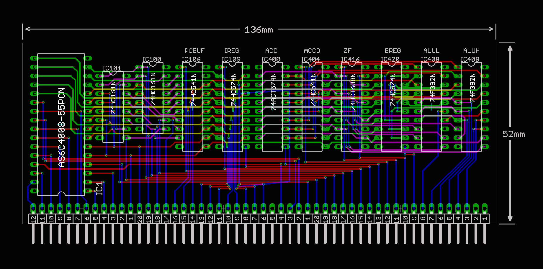
Here is my current version of an 8-bit slice board:
A kind of fake view
Just top and bottom shown:
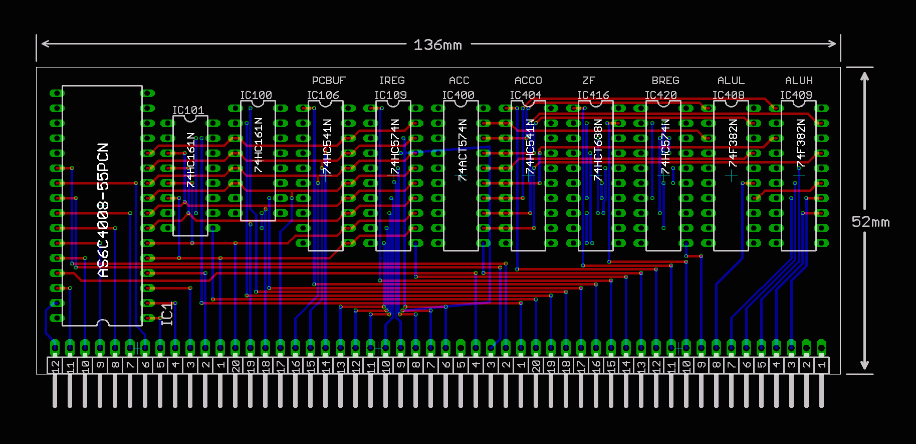
All layers
The quote from pcbway.com for this design is $ 224 (€ 190) including shiping to Germany. I would probably need to have to pay 16% VAT, which would make it (sic!} € 220. This might seem much, but I save quite some time and hair by not attempting to build that on a bread board.
Before letting this board made, I will turn the netlist as the ECAD application has it into a Verilog model and put together four slices and my current control logic and see that the resulting machines behaves.
I want pull-ups on the address and data lines. Perhaps I add these to the layout? Not sure.
Also I want a legend on the connector.
The plan is to hook this board up to some other machine with the 49 needed GPIO lines. More are needed, when hooking up four of them. This other machine then would play the rôle of the control logic. We have full control about the slices and could make the bus float and access the SRAM to upload some programm.
We need to figure this out.
In this board A[7:0] are connected to A[7:0] of the SRAM, the rest
A[19:8] is on the connector. This might seem strange at first. But
remember that you could permute the address lines as you wish. We just
pretend, that the second slice would drive A[15:8]. Likewise for the
third. The fourth will not contribute any addresses, as our address
bus is only 24 bits wide.
However we only have 19 address lines on our SRAM. So the third
slice already cannot apply A[23:16] to the RAM, only A[18:16].
A connection scheme would be like this
    real            slice 0         slice 1         slice 2         slice 3
    A[7:0]          A[7:0]          A[15:8]         A[23:16]        A[31:24]
    A[15:0]         A[15:0]         A[7:0]          A[23:16]        A[31:24]
    A[23:16]        A[23:16]        A[15:0]         A[7:0]          A[31:24]
    A[31:24]        A[31:24]        A[31:24]        A[31:24]        A[7:0]
Since we don't have A[31:24]:
    real            slice 0         slice 1         slice 2         slice 3
    A[7:0]          A[7:0]          A[15:8]         A[23:16]        A[31:24]
    A[15:0]         A[15:0]         A[7:0]          A[23:16]        A[31:24]
    A[23:16]        A[23:16]        A[15:0]         A[7:0]          --
    A[31:24]        --              --              --              A[7:0]
The consequence is, that we need solder jumpers of the output of both the instruction register and the PC towards the bus. As for the third and foruth slice those signals need to be applied from outside. I could be a cowboy here and just cut the relevant pins. And on the fourth slice the PC buffer isn't populated anyway.
This would be fine, wouldn't it be for us needing to get at the opcode, which is in the fourth instruction register. More solder jumpers. Tomorrow!
--
Gilbert Baumann