The purpose is to build a 32-bit CPU from TTL (74xx) ICs. The instruction set archiecture (ISA) is one-address and inspired by the early designs in the 50s and the EDVAC.
Our design features only a program counter and an accumulator and no other registers. Each instruction occupies a whole word and has an opcode part and an address part. Generally the address part specifies the address where to find the second operand besides the accumulator.
For conditional branching an overflow flag (OV) and a carry flag (CF) are provided. The CF is set when the result of an addition or subtraction seen as unsigned arithmetic does not fit 32 bit. The OV indicates whether the result, when interpreted as signed arithmetic, would overflow. Branching on the accumulator not being zero also is provided, but there is no separate zero flag.
The instruction set is quite simple and only has 12 instructions.
32      28      24                            0
+--------+-------+----------------------------+
| opcode | spare |       addr                 |
+--------+-------+----------------------------+
opcode   instruction     action
-----------------------------------------------------------
0        add <addr>      A = A + [addr] ;CF, OV affected
1        undefined
2        sub <addr>      A = A - [addr] ;CF, OV affected
3        undefined

4        ior <addr>      A = A | [addr] ;CF, OV undefined
5        xor <addr>      A = A ^ [addr] ;CF, OV undefined
6        and <addr>      A = A & [addr] ;CF, OV undefined
7        asr 1           A = A >> 1     ;CF, OV undefined

8        lod <addr>      A = [addr]
9        undefined
A        sto <addr>      [addr] = A
B        undefined

C        jmp <addr>      PC = addr
D        jnz <addr>      PC = addr, if A != 0
E        jnc <addr>      PC = addr, if CF clear
F        jnv <addr>      PC = addr, if OV clear
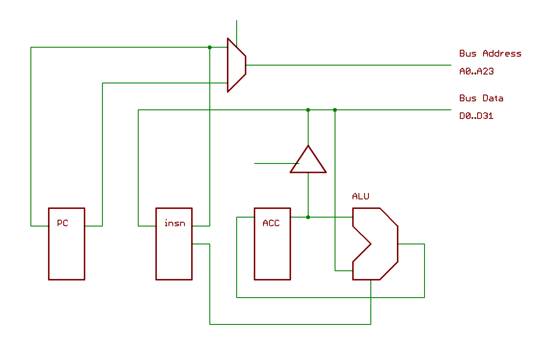
Here is a simplified block diagram of the machine:
We have three registers: program counter (PC), instruction register (INSN), accumulator (ACC),
PC: The program counter could output its value to the bus address and be loaded from the instruction register.
INSN: The instruction register is loaded from bus data. The address part of an instruction could be output to the bus address. The opcode part is in concept the function the ALU has to perform. But some decoding needs to take place (not shown).
ACC: The accumulator always places its value on the ALU A input. It
may also for the sto instruction being placed onto the data bus. The
accumulator is always loaded through the ALU. For lod the ALU will
perform F=B, and for jumps it will perform F=A and thus not altering
the accumulator value.
The machine follows a strict constant sequence. First the instruction
is loaded and then the address part of the instruction becomes the bus
address and the instruction is executed. For the arithmetic/logic
instructions and load a read cycle is initiated. For sto a write
cycle is generated. On jumps neither a read or write cycle is issued.
Each bus transfer takes four cycles. We prefer clean bus transfers, so for a read we first apply the bus address and then let a cycle pass for the address to settle on the address lines. Only then we pull /RD. After another cycle we clock tthe data into what ever register needs it. In fact it is only the INSN register and then the B register. The ACC is never loaded directly from the bus.
BA          <--- PC -------> <--- INSN -----> <--- PC -------> <--- INSN ----->

/RD         ----________---- ----________---- ----________---- ----________----

CLK_INSN    ________----____ ________________ ________----____ ________________

CLK_B       ________________ ________----____ ________________ ________----____

CLK_PC      ----____________ ________________ ----____________ ________________

                                         < .......................... >
add, sub, ior, xor, andWe will use the '381/'382 4-bit ALU
chip plus the '182 carry
lookahead generator to implement
the arithmetic and logic functions add, sub, ior, xor, and
and.
The '381/'382 is a four bit ALU in a nice 20-pin package. Beside the carry flag it also generates the overflow flag. Carry propagate and generate outputs are provided for carry lookahead, which we use with the '181 chip. The only odd thing is, that subtraction has the interpretation: CF=1 is no borrow and CF=0 is borrow. Hence in contrast to the addition we would need to pass in CF=1 instead of CF=0.
Three '381 one '382 and one '181 form a 16-bit ALU as shown in the Fairchild datasheet for the '382:
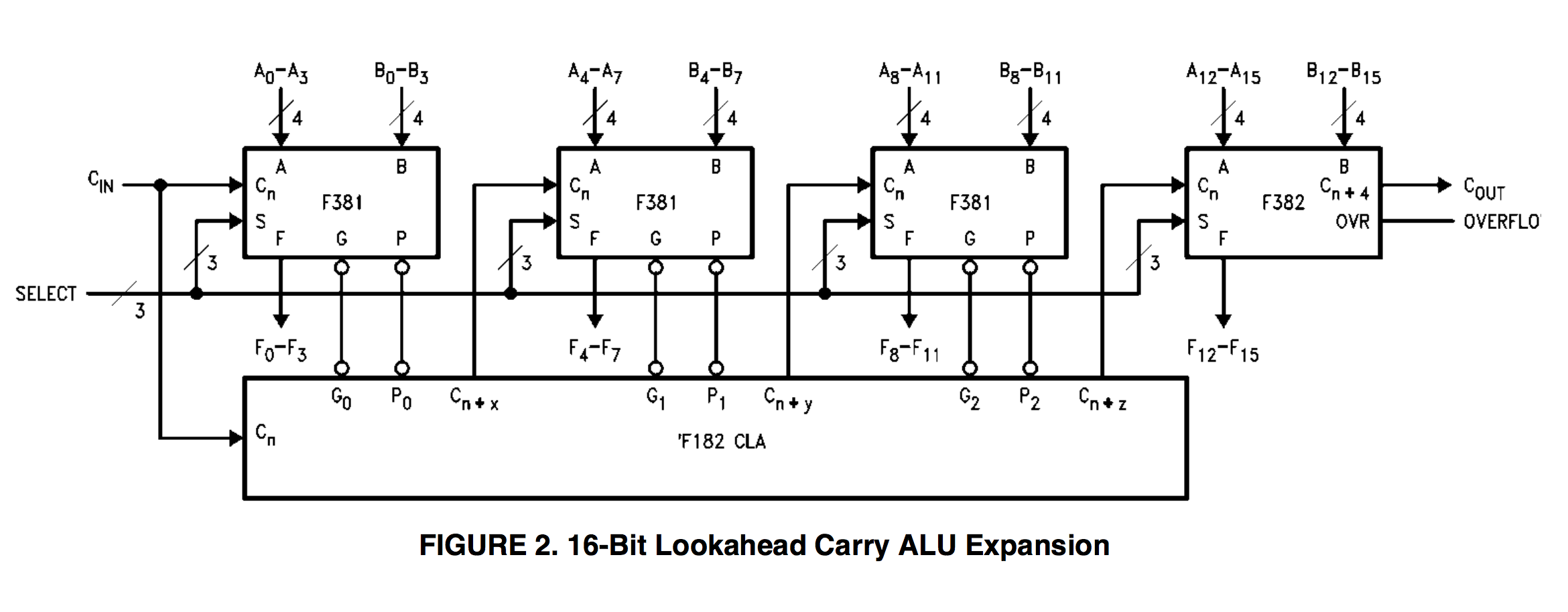
What is not shown is that the '182 also provides /P and /G output,
so we could combine two those 16-bit ALU with another '182 to form our
32-bit ALU.
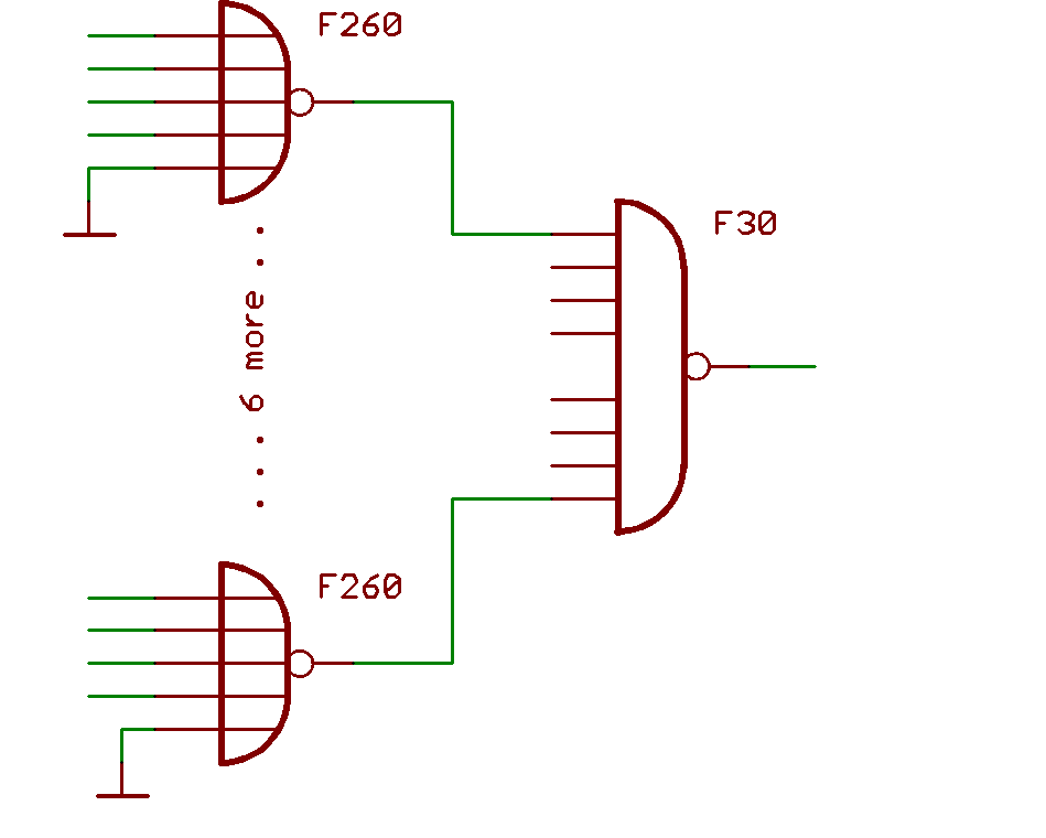
In theory we use a 32-input NOR-gate. But there is no such thing. But
there is the '25 dual 4-input NOR gate. We
use eight of those gates, four chips, to get a partial zero detection
for the result in group of four bits. We yield eight lines that all
will be H when the whole word is zero.
Note: We are not quite sure that the 74F25 ever existed, but there is 74F260 dual 5-input NOR gate, which we could use instead. The good news it is still active (2020) and available from e.g. Texas Instruments.
What we now need is an 8-input AND gate. There is the 8-input NAND
gate '30 which we could use instead. This
leads to the zero flag being inverted, L meanning zero detected and
H otherwise. We don't bother much about that as the zero flag only
used internally.
The schematic would look like this:
The total progagation delay using F series devices is 12.1ns (6.6ns + 5.5ns).
Here is our design of the external bus interface. All bus lines have pull-up resistors to keep it from floating.
A[23:0]
Address lines. We could address 16M words. Though I/O is memory mapped.
D[31:0]
32 bit data to be transfered.
/RD
/WR/READY
/HALT
Open-collector line. A L here is a request for the CPU to let go
of the bus and halt. The currently executing instruction however
will finish until this happens. The halt request is acknowledged by
/HACK.
When this happens all bus lines are in a high-Z state and another party could use the bus.
/HACK
/RESET
Open-collector line. This is an asyncrounous reset. While in reset
A[23:0], D[31:0], /RD, /WR are in in high-Z state only kept
by pullups from flowing. When /RESET goes high again the CPU
would start executing instructions from 0x000000.
CLK
In the ROM is a monitor, which allows you to inspect memory, and to branch to a certain address. Furthermore one could read and write to the disk as well as to boot from the disk.
Commands
G addr
Branch to addr.
R [addr]
Show memory from address addr on. When addr is
not provided the end of the last S output is taken.
D [addr]
Disassmble from address addr on. When addr is
not provided the end of the last D output is taken.
ZU addr len
Initiate a Z-modem transfer from the system to
the TTY.
ZD addr
Initiate a Z-modem transfer from the TTY to the system.
Different technologies have different output voltages for a low level
signal (L) and a high level signal (H). Likewise the thresholds to
detect a L or a H are different. You cannot in general expect to
be able to mix technologies and expect this to work.
While e.g. the modern HC technology outputs are almost rail-to-rail, outputs of TTL or F are not. E.g. An 'F device will only output 2.5V for a high level.
    HCT     HC      F
OL  0.1     0.1     0.5
IL  1.2     2.1     0.8

OH  5.0     5.0     2.5
IH  1.6     2.4     2.0